CCE4501 Mini Evaluation Board
FREE SHIPPING U.S. 48
In house technical support provided for all Creative Chips products!
General Information
Power Supply
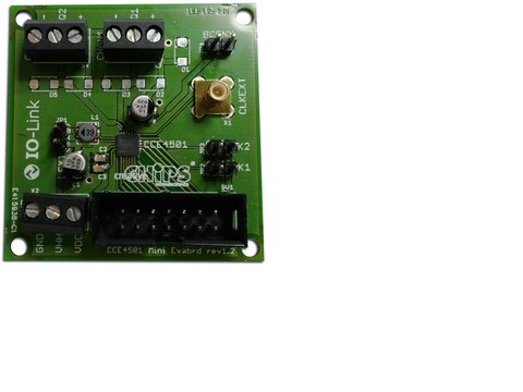
The L+ voltage of the CCE4501 is applied through the terminal CHAN1 or CHAN2, where L+ can be 9-30 V. The VHH voltage is applied through the terminal PWR, where VHH can be 7-30 V. If the DC/DCconverter of the CCE4501 is active, the 7 V VHH voltage will be generated independently, usingthe L+ voltage.
The CCE4501 additionally integrates a low drop voltage regulator that generates a selectable voltage VDD that can be 3.3 V or 5 V. This voltage is used as digital pad supply, but can be also used for the supply of external components. In case of the evaluation board, the VDD is programmed as 3.3 V.
DC/DC Converter
To enable the integrated DC/DC converter the coil needs to be connected using jumper LEXT and BC_ENX pin must be pulled to ground using jumper BCENX. If the DC/DC converter is disabled, the coil must not be connected to avoid damage to the evaluation board.
Oscillator
The internal RC oscillator of the CCE4501 is active while K1 and K2 are left open. It can be measured at the CLKEXT terminal.To clock the CCE4501 over an external source, the jumper K2 needs to be closed. An externalclock of 3.6864 MHz can be at the CLKEXT terminal.
External Connector
The digital pins of the CCE4501 are accessed via the CTRL connector.
Downloads
Datasheet |
|||
| File | Size | Modified | |
|---|---|---|---|
 |
CCE4501 Mini Evaluation Board | 345.00kB | 09-JUN-2016 |
Documentation |
|||
| File | Size | Modified | |
|
CCE4501 Datasheet | 779.00kB | 09-JUN-2106 |
|
|
|